Lab-on-a-chip (LOC) technology utilized every day for mission-critical point-of-care applications, clinical diagnostics, drug discovery, and boundless other applications depend on microfluidic chips. Settling on a functional, manufacturable design for your microfluidic chip that ensures both reliable performance in the field and cost-effective production is one of the most challenging aspects of lab-on-a-chip product design.
One of the many deciding factors influencing reliability and cost-effectiveness in a chip’s design is the polymer bonding process utilized in its manufacture. From laser welding to ultrasonic welding to solvent and adhesive film bonding to thermal fusion bonding, a manufacturer has many options to choose from, each with its own advantages and disadvantages, as well as its own ideal use case.
In our new whitepaper, you’ll learn what sets these polymer bonding processes apart from one another and how to make an informed choice regarding which is best for your needs.
Why the Right Bonding Process Matters
Choosing the right polymer bonding process to bring your chip from the design bench to a finished product requires careful consideration of the material composition, design, and intended purpose of your microfluidic chip.
Your choice of bonding process impacts not only the effectiveness of your chip’s design for its intended purpose but its ability to be manufactured at your desired scale within your budget.
Other crucial factors in your chip design also heavily depend on your choice of bonding process—such as:
- Reproducibility – minimizing part-to-part variation
- Cost-per-unit
- Fabrication yield and throughput—certain bonding processes are slower than others or are more conducive to automation
- Whether or not your production process will require additional processing steps and facilities
Learn How to Weld Plastic Together for Microfluidic Products in Our New Free White Paper
In our new technical resource, you’ll find a comprehensive overview of available polymer bonding processes for microfluidic chip design, with a focus on Transparent “Clear-to-Clear” Laser Plastic Welding. Topics covered include:
- Factors to consider when choosing a polymer bonding process
- High-level overviews of the common polymer bonding processes
- Advantages and disadvantages of each polymer bonding process, including use cases for laser welding and ultrasonic welding plastic
- A case study on the use and effectiveness of laser plastic welding for lab-on-a-chip designs
What Is Transparent Laser Plastic Welding?
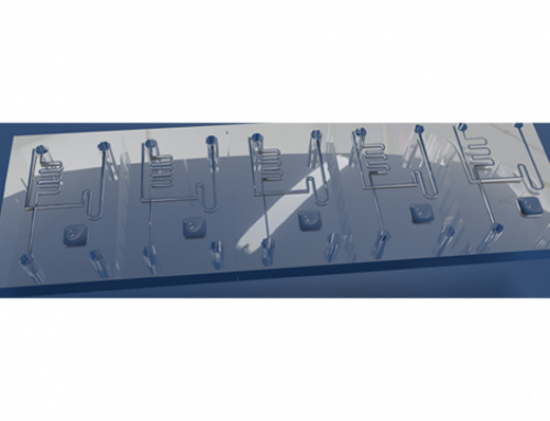
Medical microfluidic devices frequently use laser welding for plastic, which applies energy to melt two substrates together by heating them close to the materials’ glass transition temperature. The bond created is as strong as the base material.
Commonly, laser welding involves welding transparent plastic to black plastic, which is not always desirable for certain LOC applications. As its name suggests, Transparent Laser Plastic Welding, also known as Clear-to-Clear welding, welds together transparent plastics to retain optical transparency throughout the chip.
The attributes of Clear-to-Clear welding include:
- Optical transparency
- Contour welding paths
- An automation-friendly application process
- Short cycle times
Transparent Laser Plastic Welding provides a strong bond between dissimilar materials without the need for absorber material additives. Taking into account laser welding’s tight tolerances and ease of automation as well, optical transparency makes Transparent Laser Plastic Welding particularly useful for chips requiring precise alignment with vision systems.
Keep Up-To-Date With Developments in Microfluidics
Microfluidics technology advances every day. At the micro-scale of microfluidic chips, the devil is in the details, and little details often have massive ramifications. It can be difficult to keep track of everything you need to know in the world of lab-on-a-chip product design and development.
At Vantiva Precision BioDevices, we continue to develop and publish useful digital resources to help you keep up-to-date with best practices in the realm of microfluidics. From our Rapid Prototyping Design Guide to our case studies and white papers, our resources provide you with the expertise you need to make the right decisions to bring your lab-on-a-chip product idea to life.
To keep you up-to-date with the rapidly changing world of microfluidics manufacturing and design, we offer an email industry newsletter to keep you updated on the latest developments at Vantiva Precision BioDevices and in the microfluidics industry as a whole.
You’ll also be the first to know whenever we publish a new digital resource such as this Laser Welding white paper or our other white papers and case studies.
To stay on the cutting edge of microfluidics, sign up today:
Ready to Bring Your Lab-on-a-Chip Ideas to Life?
Transferring your idea for a microfluidic chip design from the bench to an injection-molding process to a viable product can be a challenge without the right tools and expertise on your side.
Vantiva Precision BioDevices leverages a 100-year legacy of technological and logistics expertise to take the risk out of microfluidic chip design, assembly, scale-up, and distribution. We’re here to provide the support you need at any step of the design, prototyping, or production process to help you refine and realize your Lab-on-a-Chip product for manufacturability and cost-effectiveness at any scale.
Schedule a consultation with our expert microfluidics engineers to find out more about what we can do to help you bring your product to life as your strategic partner.